EDB: Layout Creation and Setup#
This example demonstrates how to to
Create a layout layer stackup.
Define padstacks.
Place padstack instances in the layout where the connectors are located.
Create primitives such as polygons and traces.
Create “components” from the padstack definitions using “pins”. >The “component” in EDB acts as a placeholder to enable automatic >placement of electrical models, or >as in this example to assign ports. In many >cases the EDB is imported from a 3rd party layout, in which case the >concept of a “component” as a placeholder is needed to map >models to the components on the PCB for later use in the >simulation.
Create the HFSS simulation setup and assign ports where the connectors are located.
View PCB trace model#
Here is an image of the model that is created in this example.
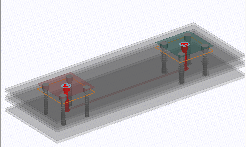
The rectangular sheets at each end of the PCB enable placement of ports where the connectors are located.
Initialize the EDB layout object.
[1]:
import os
import tempfile

import pyaedt

from pyedb import Edb

temp_dir = tempfile.TemporaryDirectory(suffix=".ansys")
aedb_path = os.path.join(temp_dir.name, "component_example.aedb")

# Select EDB version (change it manually if needed, e.g. "2024.1")
edb_version = "2024.1"
print(f"EDB version: {edb_version}")

edb = Edb(edbpath=aedb_path, edbversion=edb_version)
print("EDB is located at {}".format(aedb_path))
EDB version: 2024.1
PyAEDT INFO: Logger is initialized in EDB.
PyAEDT INFO: legacy v0.21.1
PyAEDT INFO: Python version 3.10.11 (tags/v3.10.11:7d4cc5a, Apr  5 2023, 00:38:17) [MSC v.1929 64 bit (AMD64)]
PyAEDT INFO: EDB C:\Users\ansys\AppData\Local\Temp\tmpic2z03wz.ansys\component_example.aedb created correctly.
PyAEDT INFO: EDB initialized.
EDB is located at C:\Users\ansys\AppData\Local\Temp\tmpic2z03wz.ansys\component_example.aedb
Initialize variables
[2]:
layout_count = 12
diel_material_name = "FR4_epoxy"
diel_thickness = "0.15mm"
cond_thickness_outer = "0.05mm"
cond_thickness_inner = "0.017mm"
soldermask_thickness = "0.05mm"
trace_in_layer = "TOP"
trace_out_layer = "L10"
trace_width = "200um"
connector_size = 2e-3
conectors_position = [[0, 0], [10e-3, 0]]
Create the stackup
[3]:
edb.stackup.create_symmetric_stackup(
    layer_count=layout_count,
    inner_layer_thickness=cond_thickness_inner,
    outer_layer_thickness=cond_thickness_outer,
    soldermask_thickness=soldermask_thickness,
    dielectric_thickness=diel_thickness,
    dielectric_material=diel_material_name,
)
Material 'copper' does not exist in material library. Intempt to create it from syslib.
Material 'FR4_epoxy' does not exist in material library. Intempt to create it from syslib.
Material 'SolderMask' does not exist in material library. Intempt to create it from syslib.
[3]:
True
Create ground planes
[4]:
ground_layers = [
    layer_name for layer_name in edb.stackup.signal_layers.keys() if layer_name not in [trace_in_layer, trace_out_layer]
]
plane_shape = edb.modeler.Shape("rectangle", pointA=["-3mm", "-3mm"], pointB=["13mm", "3mm"])
for i in ground_layers:
    edb.modeler.create_polygon(plane_shape, i, net_name="VSS")
Add design parameters#
Parameters that are preceded by a “$” character have project-wide scope. Therefore, the padstack definition and hence all instances of that padstack rely on the parameters.
Parameters such as “trace_in_width” and “trace_out_width” have local scope and are only used in in the design.
[5]:
edb.add_design_variable("$via_hole_size", "0.3mm")
edb.add_design_variable("$antipaddiam", "0.7mm")
edb.add_design_variable("$paddiam", "0.5mm")
edb.add_design_variable("trace_in_width", "0.2mm", is_parameter=True)
edb.add_design_variable("trace_out_width", "0.1mm", is_parameter=True)
[5]:
(True, <Ansys.Ansoft.Edb.Utility.VariableServer object at 0x000002431C7B2070>)
Create the connector component#
The component definition is used to place the connector on the PCB. First define the padstacks.
[6]:
edb.padstacks.create_padstack(
    padstackname="Via", holediam="$via_hole_size", antipaddiam="$antipaddiam", paddiam="$paddiam"
)
PyAEDT INFO: Padstack Via create correctly
[6]:
'Via'
Create the first connector
[7]:
component1_pins = [
    edb.padstacks.place_padstack(
        conectors_position[0],
        "Via",
        net_name="VDD",
        fromlayer=trace_in_layer,
        tolayer=trace_out_layer,
    ),
    edb.padstacks.place_padstack(
        [
            conectors_position[0][0] - connector_size / 2,
            conectors_position[0][1] - connector_size / 2,
        ],
        "Via",
        net_name="VSS",
    ),
    edb.padstacks.place_padstack(
        [
            conectors_position[0][0] + connector_size / 2,
            conectors_position[0][1] - connector_size / 2,
        ],
        "Via",
        net_name="VSS",
    ),
    edb.padstacks.place_padstack(
        [
            conectors_position[0][0] + connector_size / 2,
            conectors_position[0][1] + connector_size / 2,
        ],
        "Via",
        net_name="VSS",
    ),
    edb.padstacks.place_padstack(
        [
            conectors_position[0][0] - connector_size / 2,
            conectors_position[0][1] + connector_size / 2,
        ],
        "Via",
        net_name="VSS",
    ),
]
Create the second connector
[8]:
component2_pins = [
    edb.padstacks.place_padstack(
        conectors_position[-1],
        "Via",
        net_name="VDD",
        fromlayer=trace_in_layer,
        tolayer=trace_out_layer,
    ),
    edb.padstacks.place_padstack(
        [
            conectors_position[1][0] - connector_size / 2,
            conectors_position[1][1] - connector_size / 2,
        ],
        "Via",
        net_name="VSS",
    ),
    edb.padstacks.place_padstack(
        [
            conectors_position[1][0] + connector_size / 2,
            conectors_position[1][1] - connector_size / 2,
        ],
        "Via",
        net_name="VSS",
    ),
    edb.padstacks.place_padstack(
        [
            conectors_position[1][0] + connector_size / 2,
            conectors_position[1][1] + connector_size / 2,
        ],
        "Via",
        net_name="VSS",
    ),
    edb.padstacks.place_padstack(
        [
            conectors_position[1][0] - connector_size / 2,
            conectors_position[1][1] + connector_size / 2,
        ],
        "Via",
        net_name="VSS",
    ),
]
Define pins#
Pins are fist defined to allow a component to subsequently connect to the remainder of the model. In this case, ports are assigned at the connector instances using the pins.
[9]:
for padstack_instance in list(edb.padstacks.instances.values()):
    padstack_instance.is_pin = True
Create components from the pins
[10]:
edb.components.create(component1_pins, "connector_1")
edb.components.create(component2_pins, "connector_2")
[10]:
<pyedb.dotnet.edb_core.cell.hierarchy.component.EDBComponent at 0x2431c3a69b0>
Create ports on the pins and insert a simulation setup using the SimulationConfiguration class.
[11]:
sim_setup = edb.new_simulation_configuration()
sim_setup.solver_type = sim_setup.SOLVER_TYPE.Hfss3dLayout
sim_setup.batch_solve_settings.cutout_subdesign_expansion = 0.01
sim_setup.batch_solve_settings.do_cutout_subdesign = False
sim_setup.batch_solve_settings.signal_nets = ["VDD"]
sim_setup.batch_solve_settings.components = ["connector_1", "connector_2"]
sim_setup.batch_solve_settings.power_nets = ["VSS"]
sim_setup.ac_settings.start_freq = "0GHz"
sim_setup.ac_settings.stop_freq = "5GHz"
sim_setup.ac_settings.step_freq = "1GHz"
edb.build_simulation_project(sim_setup)
PyAEDT INFO: Building simulation project.
PyAEDT INFO: Deleting existing ports.
PyAEDT INFO: Creating HFSS ports for signal nets.
PyAEDT INFO: Number of ports: 2
PyAEDT INFO: Configure HFSS extents.
PyAEDT INFO: Adding frequency sweep
PyAEDT INFO: EDB file save time: 0.00ms
[11]:
True
Save the EDB and open it in the 3D Layout editor. If non_graphical==False, there may be a delay while AEDT starts.
[12]:
edb.save_edb()
edb.close_edb()
h3d = pyaedt.Hfss3dLayout(
    specified_version="2024.1",
    projectname=aedb_path,
    non_graphical=False,  # Set non_graphical = False to launch AEDT in graphical mode.
    new_desktop_session=True,
)
PyAEDT INFO: EDB file save time: 15.57ms
PyAEDT INFO: EDB file release time: 0.00ms
PyAEDT WARNING: Argument `projectname` is deprecated for method `__init__`; use `project` instead.
PyAEDT WARNING: Argument `specified_version` is deprecated for method `__init__`; use `version` instead.
PyAEDT WARNING: Argument `new_desktop_session` is deprecated for method `__init__`; use `new_desktop` instead.
PyAEDT INFO: Initializing new Desktop session.
PyAEDT INFO: StdOut is enabled
PyAEDT INFO: Log on file is enabled
PyAEDT INFO: Log on Desktop Message Manager is enabled
PyAEDT INFO: Debug logger is disabled. PyAEDT methods will not be logged.
PyAEDT INFO: Launching PyAEDT outside AEDT with gRPC plugin.
PyAEDT INFO: New AEDT session is starting on gRPC port 65235
PyAEDT INFO: AEDT installation Path C:\Program Files\AnsysEM\v241\Win64
PyAEDT INFO: Ansoft.ElectronicsDesktop.2024.1 version started with process ID 5088.
PyAEDT INFO: pyaedt v0.9.9
PyAEDT INFO: Python version 3.10.11 (tags/v3.10.11:7d4cc5a, Apr  5 2023, 00:38:17) [MSC v.1929 64 bit (AMD64)]
PyAEDT INFO: AEDT 2024.1.0 Build Date 2023-11-27 22:16:18
PyAEDT INFO: EDB folder C:\Users\ansys\AppData\Local\Temp\tmpic2z03wz.ansys\component_example.aedb has been imported to project component_example
PyAEDT INFO: Active Design set to Cell_QN9D1A
PyAEDT INFO: Aedt Objects correctly read
Release the application from the Python kernel#
It is important to release the application from the Python kernel after execution of the script. The default behavior of the release_desktop() method closes all open projects and closes the application.
If you want to conintue working on the project in graphical mode after script execution, call the following method with both arguments set to False.
[13]:
h3d.release_desktop(close_projects=True, close_desktop=True)
PyAEDT INFO: Desktop has been released and closed.
[13]:
True
Clean up the temporary directory#
The following command cleans up the temporary directory, thereby removing all project files. If you’d like to save this project, save it to a folder of your choice prior to running the following cell.
[14]:
temp_dir.cleanup()