EDB: geometry creation#
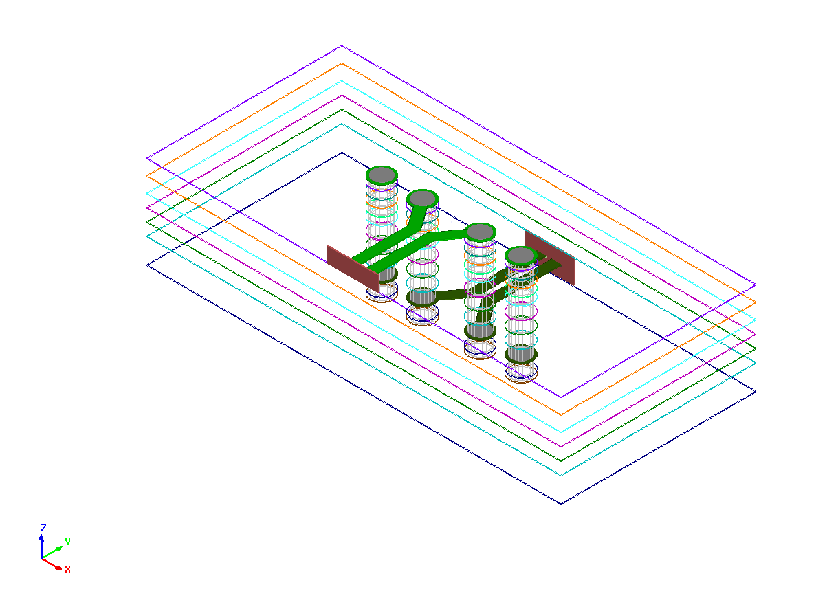
This example shows how you can use EDB to create a layout. ## Final expected project
Import EDB layout object#
Import the EDB layout object and initialize it on version 2023 R2.
[1]:
import os
import tempfile

import pyedb

temp_dir = tempfile.TemporaryDirectory(suffix=".ansys")
aedb_path = os.path.join(temp_dir.name, "create_via.aedb")
print(f"AEDB file path: {aedb_path}")

# Select EDB version (change it manually if needed, e.g. "2024.2")
edb_version = "2024.2"
print(f"EDB version: {edb_version}")

edb = pyedb.Edb(edbpath=aedb_path, edbversion=edb_version)
AEDB file path: C:\Users\ansys\AppData\Local\Temp\tmprv6cj7av.ansys\create_via.aedb
EDB version: 2024.2
PyEDB INFO: StdOut is enabled
PyEDB INFO: Logger is initialized in EDB.
PyEDB INFO: legacy v0.34.3
PyEDB INFO: Python version 3.10.11 (tags/v3.10.11:7d4cc5a, Apr  5 2023, 00:38:17) [MSC v.1929 64 bit (AMD64)]
--- Logging error ---
Traceback (most recent call last):
  File "C:\actions-runner\_work\_tool\Python\3.10.11\x64\lib\logging\handlers.py", line 74, in emit
    self.doRollover()
  File "C:\actions-runner\_work\_tool\Python\3.10.11\x64\lib\logging\handlers.py", line 179, in doRollover
    self.rotate(self.baseFilename, dfn)
  File "C:\actions-runner\_work\_tool\Python\3.10.11\x64\lib\logging\handlers.py", line 115, in rotate
    os.rename(source, dest)
PermissionError: [WinError 32] The process cannot access the file because it is being used by another process: 'C:\\Users\\ansys\\AppData\\Local\\Temp\\pyedb_ansys.log' -> 'C:\\Users\\ansys\\AppData\\Local\\Temp\\pyedb_ansys.log.1'
Call stack:
  File "C:\actions-runner\_work\_tool\Python\3.10.11\x64\lib\runpy.py", line 196, in _run_module_as_main
    return _run_code(code, main_globals, None,
  File "C:\actions-runner\_work\_tool\Python\3.10.11\x64\lib\runpy.py", line 86, in _run_code
    exec(code, run_globals)
  File "C:\actions-runner\_work\pyedb\pyedb\.venv\lib\site-packages\ipykernel_launcher.py", line 18, in <module>
    app.launch_new_instance()
  File "C:\actions-runner\_work\pyedb\pyedb\.venv\lib\site-packages\traitlets\config\application.py", line 1075, in launch_instance
    app.start()
  File "C:\actions-runner\_work\pyedb\pyedb\.venv\lib\site-packages\ipykernel\kernelapp.py", line 739, in start
    self.io_loop.start()
  File "C:\actions-runner\_work\pyedb\pyedb\.venv\lib\site-packages\tornado\platform\asyncio.py", line 205, in start
    self.asyncio_loop.run_forever()
  File "C:\actions-runner\_work\_tool\Python\3.10.11\x64\lib\asyncio\base_events.py", line 603, in run_forever
    self._run_once()
  File "C:\actions-runner\_work\_tool\Python\3.10.11\x64\lib\asyncio\base_events.py", line 1909, in _run_once
    handle._run()
  File "C:\actions-runner\_work\_tool\Python\3.10.11\x64\lib\asyncio\events.py", line 80, in _run
    self._context.run(self._callback, *self._args)
  File "C:\actions-runner\_work\pyedb\pyedb\.venv\lib\site-packages\ipykernel\kernelbase.py", line 545, in dispatch_queue
    await self.process_one()
  File "C:\actions-runner\_work\pyedb\pyedb\.venv\lib\site-packages\ipykernel\kernelbase.py", line 534, in process_one
    await dispatch(*args)
  File "C:\actions-runner\_work\pyedb\pyedb\.venv\lib\site-packages\ipykernel\kernelbase.py", line 437, in dispatch_shell
    await result
  File "C:\actions-runner\_work\pyedb\pyedb\.venv\lib\site-packages\ipykernel\ipkernel.py", line 362, in execute_request
    await super().execute_request(stream, ident, parent)
  File "C:\actions-runner\_work\pyedb\pyedb\.venv\lib\site-packages\ipykernel\kernelbase.py", line 778, in execute_request
    reply_content = await reply_content
  File "C:\actions-runner\_work\pyedb\pyedb\.venv\lib\site-packages\ipykernel\ipkernel.py", line 449, in do_execute
    res = shell.run_cell(
  File "C:\actions-runner\_work\pyedb\pyedb\.venv\lib\site-packages\ipykernel\zmqshell.py", line 549, in run_cell
    return super().run_cell(*args, **kwargs)
  File "C:\actions-runner\_work\pyedb\pyedb\.venv\lib\site-packages\IPython\core\interactiveshell.py", line 3075, in run_cell
    result = self._run_cell(
  File "C:\actions-runner\_work\pyedb\pyedb\.venv\lib\site-packages\IPython\core\interactiveshell.py", line 3130, in _run_cell
    result = runner(coro)
  File "C:\actions-runner\_work\pyedb\pyedb\.venv\lib\site-packages\IPython\core\async_helpers.py", line 128, in _pseudo_sync_runner
    coro.send(None)
  File "C:\actions-runner\_work\pyedb\pyedb\.venv\lib\site-packages\IPython\core\interactiveshell.py", line 3334, in run_cell_async
    has_raised = await self.run_ast_nodes(code_ast.body, cell_name,
  File "C:\actions-runner\_work\pyedb\pyedb\.venv\lib\site-packages\IPython\core\interactiveshell.py", line 3517, in run_ast_nodes
    if await self.run_code(code, result, async_=asy):
  File "C:\actions-runner\_work\pyedb\pyedb\.venv\lib\site-packages\IPython\core\interactiveshell.py", line 3577, in run_code
    exec(code_obj, self.user_global_ns, self.user_ns)
  File "C:\Users\ansys\AppData\Local\Temp\ipykernel_3956\450015450.py", line 14, in <module>
    edb = pyedb.Edb(edbpath=aedb_path, edbversion=edb_version)
  File "C:\actions-runner\_work\pyedb\pyedb\.venv\lib\site-packages\pyedb\generic\design_types.py", line 110, in Edb
    return app(
  File "C:\actions-runner\_work\pyedb\pyedb\.venv\lib\site-packages\pyedb\dotnet\edb.py", line 196, in __init__
    Database.__init__(self, edbversion=edbversion, student_version=student_version)
  File "C:\actions-runner\_work\pyedb\pyedb\.venv\lib\site-packages\pyedb\dotnet\edb_core\dotnet\database.py", line 802, in __init__
    EdbDotNet.__init__(self, edbversion=edbversion, student_version=student_version)
  File "C:\actions-runner\_work\pyedb\pyedb\.venv\lib\site-packages\pyedb\dotnet\edb_core\dotnet\database.py", line 703, in __init__
    self._logger.enable_stdout_log()
  File "C:\actions-runner\_work\pyedb\pyedb\.venv\lib\site-packages\pyedb\edb_logger.py", line 318, in enable_stdout_log
    self.info("StdOut is enabled")
  File "C:\actions-runner\_work\pyedb\pyedb\.venv\lib\site-packages\pyedb\edb_logger.py", line 346, in info
    return self._log_on_handler(0, msg, *args, **kwargs)
  File "C:\actions-runner\_work\pyedb\pyedb\.venv\lib\site-packages\pyedb\edb_logger.py", line 293, in _log_on_handler
    self._global.info(message_text, *args, **kwargs)
Message: 'StdOut is enabled'
Arguments: ()
--- Logging error ---
Traceback (most recent call last):
  File "C:\actions-runner\_work\_tool\Python\3.10.11\x64\lib\logging\handlers.py", line 74, in emit
    self.doRollover()
  File "C:\actions-runner\_work\_tool\Python\3.10.11\x64\lib\logging\handlers.py", line 179, in doRollover
    self.rotate(self.baseFilename, dfn)
  File "C:\actions-runner\_work\_tool\Python\3.10.11\x64\lib\logging\handlers.py", line 115, in rotate
    os.rename(source, dest)
PermissionError: [WinError 32] The process cannot access the file because it is being used by another process: 'C:\\Users\\ansys\\AppData\\Local\\Temp\\pyedb_ansys.log' -> 'C:\\Users\\ansys\\AppData\\Local\\Temp\\pyedb_ansys.log.1'
Call stack:
  File "C:\actions-runner\_work\_tool\Python\3.10.11\x64\lib\runpy.py", line 196, in _run_module_as_main
    return _run_code(code, main_globals, None,
  File "C:\actions-runner\_work\_tool\Python\3.10.11\x64\lib\runpy.py", line 86, in _run_code
    exec(code, run_globals)
  File "C:\actions-runner\_work\pyedb\pyedb\.venv\lib\site-packages\ipykernel_launcher.py", line 18, in <module>
    app.launch_new_instance()
  File "C:\actions-runner\_work\pyedb\pyedb\.venv\lib\site-packages\traitlets\config\application.py", line 1075, in launch_instance
    app.start()
  File "C:\actions-runner\_work\pyedb\pyedb\.venv\lib\site-packages\ipykernel\kernelapp.py", line 739, in start
    self.io_loop.start()
  File "C:\actions-runner\_work\pyedb\pyedb\.venv\lib\site-packages\tornado\platform\asyncio.py", line 205, in start
    self.asyncio_loop.run_forever()
  File "C:\actions-runner\_work\_tool\Python\3.10.11\x64\lib\asyncio\base_events.py", line 603, in run_forever
    self._run_once()
  File "C:\actions-runner\_work\_tool\Python\3.10.11\x64\lib\asyncio\base_events.py", line 1909, in _run_once
    handle._run()
  File "C:\actions-runner\_work\_tool\Python\3.10.11\x64\lib\asyncio\events.py", line 80, in _run
    self._context.run(self._callback, *self._args)
  File "C:\actions-runner\_work\pyedb\pyedb\.venv\lib\site-packages\ipykernel\kernelbase.py", line 545, in dispatch_queue
    await self.process_one()
  File "C:\actions-runner\_work\pyedb\pyedb\.venv\lib\site-packages\ipykernel\kernelbase.py", line 534, in process_one
    await dispatch(*args)
  File "C:\actions-runner\_work\pyedb\pyedb\.venv\lib\site-packages\ipykernel\kernelbase.py", line 437, in dispatch_shell
    await result
  File "C:\actions-runner\_work\pyedb\pyedb\.venv\lib\site-packages\ipykernel\ipkernel.py", line 362, in execute_request
    await super().execute_request(stream, ident, parent)
  File "C:\actions-runner\_work\pyedb\pyedb\.venv\lib\site-packages\ipykernel\kernelbase.py", line 778, in execute_request
    reply_content = await reply_content
  File "C:\actions-runner\_work\pyedb\pyedb\.venv\lib\site-packages\ipykernel\ipkernel.py", line 449, in do_execute
    res = shell.run_cell(
  File "C:\actions-runner\_work\pyedb\pyedb\.venv\lib\site-packages\ipykernel\zmqshell.py", line 549, in run_cell
    return super().run_cell(*args, **kwargs)
  File "C:\actions-runner\_work\pyedb\pyedb\.venv\lib\site-packages\IPython\core\interactiveshell.py", line 3075, in run_cell
    result = self._run_cell(
  File "C:\actions-runner\_work\pyedb\pyedb\.venv\lib\site-packages\IPython\core\interactiveshell.py", line 3130, in _run_cell
    result = runner(coro)
  File "C:\actions-runner\_work\pyedb\pyedb\.venv\lib\site-packages\IPython\core\async_helpers.py", line 128, in _pseudo_sync_runner
    coro.send(None)
  File "C:\actions-runner\_work\pyedb\pyedb\.venv\lib\site-packages\IPython\core\interactiveshell.py", line 3334, in run_cell_async
    has_raised = await self.run_ast_nodes(code_ast.body, cell_name,
  File "C:\actions-runner\_work\pyedb\pyedb\.venv\lib\site-packages\IPython\core\interactiveshell.py", line 3517, in run_ast_nodes
    if await self.run_code(code, result, async_=asy):
  File "C:\actions-runner\_work\pyedb\pyedb\.venv\lib\site-packages\IPython\core\interactiveshell.py", line 3577, in run_code
    exec(code_obj, self.user_global_ns, self.user_ns)
  File "C:\Users\ansys\AppData\Local\Temp\ipykernel_3956\450015450.py", line 14, in <module>
    edb = pyedb.Edb(edbpath=aedb_path, edbversion=edb_version)
  File "C:\actions-runner\_work\pyedb\pyedb\.venv\lib\site-packages\pyedb\generic\design_types.py", line 110, in Edb
    return app(
  File "C:\actions-runner\_work\pyedb\pyedb\.venv\lib\site-packages\pyedb\dotnet\edb.py", line 196, in __init__
    Database.__init__(self, edbversion=edbversion, student_version=student_version)
  File "C:\actions-runner\_work\pyedb\pyedb\.venv\lib\site-packages\pyedb\dotnet\edb_core\dotnet\database.py", line 802, in __init__
    EdbDotNet.__init__(self, edbversion=edbversion, student_version=student_version)
  File "C:\actions-runner\_work\pyedb\pyedb\.venv\lib\site-packages\pyedb\dotnet\edb_core\dotnet\database.py", line 709, in __init__
    self._logger.info("Logger is initialized in EDB.")
  File "C:\actions-runner\_work\pyedb\pyedb\.venv\lib\site-packages\pyedb\edb_logger.py", line 346, in info
    return self._log_on_handler(0, msg, *args, **kwargs)
  File "C:\actions-runner\_work\pyedb\pyedb\.venv\lib\site-packages\pyedb\edb_logger.py", line 293, in _log_on_handler
    self._global.info(message_text, *args, **kwargs)
Message: 'Logger is initialized in EDB.'
Arguments: ()
--- Logging error ---
Traceback (most recent call last):
  File "C:\actions-runner\_work\_tool\Python\3.10.11\x64\lib\logging\handlers.py", line 74, in emit
    self.doRollover()
  File "C:\actions-runner\_work\_tool\Python\3.10.11\x64\lib\logging\handlers.py", line 179, in doRollover
    self.rotate(self.baseFilename, dfn)
  File "C:\actions-runner\_work\_tool\Python\3.10.11\x64\lib\logging\handlers.py", line 115, in rotate
    os.rename(source, dest)
PermissionError: [WinError 32] The process cannot access the file because it is being used by another process: 'C:\\Users\\ansys\\AppData\\Local\\Temp\\pyedb_ansys.log' -> 'C:\\Users\\ansys\\AppData\\Local\\Temp\\pyedb_ansys.log.1'
Call stack:
  File "C:\actions-runner\_work\_tool\Python\3.10.11\x64\lib\runpy.py", line 196, in _run_module_as_main
    return _run_code(code, main_globals, None,
  File "C:\actions-runner\_work\_tool\Python\3.10.11\x64\lib\runpy.py", line 86, in _run_code
    exec(code, run_globals)
  File "C:\actions-runner\_work\pyedb\pyedb\.venv\lib\site-packages\ipykernel_launcher.py", line 18, in <module>
    app.launch_new_instance()
  File "C:\actions-runner\_work\pyedb\pyedb\.venv\lib\site-packages\traitlets\config\application.py", line 1075, in launch_instance
    app.start()
  File "C:\actions-runner\_work\pyedb\pyedb\.venv\lib\site-packages\ipykernel\kernelapp.py", line 739, in start
    self.io_loop.start()
  File "C:\actions-runner\_work\pyedb\pyedb\.venv\lib\site-packages\tornado\platform\asyncio.py", line 205, in start
    self.asyncio_loop.run_forever()
  File "C:\actions-runner\_work\_tool\Python\3.10.11\x64\lib\asyncio\base_events.py", line 603, in run_forever
    self._run_once()
  File "C:\actions-runner\_work\_tool\Python\3.10.11\x64\lib\asyncio\base_events.py", line 1909, in _run_once
    handle._run()
  File "C:\actions-runner\_work\_tool\Python\3.10.11\x64\lib\asyncio\events.py", line 80, in _run
    self._context.run(self._callback, *self._args)
  File "C:\actions-runner\_work\pyedb\pyedb\.venv\lib\site-packages\ipykernel\kernelbase.py", line 545, in dispatch_queue
    await self.process_one()
  File "C:\actions-runner\_work\pyedb\pyedb\.venv\lib\site-packages\ipykernel\kernelbase.py", line 534, in process_one
    await dispatch(*args)
  File "C:\actions-runner\_work\pyedb\pyedb\.venv\lib\site-packages\ipykernel\kernelbase.py", line 437, in dispatch_shell
    await result
  File "C:\actions-runner\_work\pyedb\pyedb\.venv\lib\site-packages\ipykernel\ipkernel.py", line 362, in execute_request
    await super().execute_request(stream, ident, parent)
  File "C:\actions-runner\_work\pyedb\pyedb\.venv\lib\site-packages\ipykernel\kernelbase.py", line 778, in execute_request
    reply_content = await reply_content
  File "C:\actions-runner\_work\pyedb\pyedb\.venv\lib\site-packages\ipykernel\ipkernel.py", line 449, in do_execute
    res = shell.run_cell(
  File "C:\actions-runner\_work\pyedb\pyedb\.venv\lib\site-packages\ipykernel\zmqshell.py", line 549, in run_cell
    return super().run_cell(*args, **kwargs)
  File "C:\actions-runner\_work\pyedb\pyedb\.venv\lib\site-packages\IPython\core\interactiveshell.py", line 3075, in run_cell
    result = self._run_cell(
  File "C:\actions-runner\_work\pyedb\pyedb\.venv\lib\site-packages\IPython\core\interactiveshell.py", line 3130, in _run_cell
    result = runner(coro)
  File "C:\actions-runner\_work\pyedb\pyedb\.venv\lib\site-packages\IPython\core\async_helpers.py", line 128, in _pseudo_sync_runner
    coro.send(None)
  File "C:\actions-runner\_work\pyedb\pyedb\.venv\lib\site-packages\IPython\core\interactiveshell.py", line 3334, in run_cell_async
    has_raised = await self.run_ast_nodes(code_ast.body, cell_name,
  File "C:\actions-runner\_work\pyedb\pyedb\.venv\lib\site-packages\IPython\core\interactiveshell.py", line 3517, in run_ast_nodes
    if await self.run_code(code, result, async_=asy):
  File "C:\actions-runner\_work\pyedb\pyedb\.venv\lib\site-packages\IPython\core\interactiveshell.py", line 3577, in run_code
    exec(code_obj, self.user_global_ns, self.user_ns)
  File "C:\Users\ansys\AppData\Local\Temp\ipykernel_3956\450015450.py", line 14, in <module>
    edb = pyedb.Edb(edbpath=aedb_path, edbversion=edb_version)
  File "C:\actions-runner\_work\pyedb\pyedb\.venv\lib\site-packages\pyedb\generic\design_types.py", line 110, in Edb
    return app(
  File "C:\actions-runner\_work\pyedb\pyedb\.venv\lib\site-packages\pyedb\dotnet\edb.py", line 196, in __init__
    Database.__init__(self, edbversion=edbversion, student_version=student_version)
  File "C:\actions-runner\_work\pyedb\pyedb\.venv\lib\site-packages\pyedb\dotnet\edb_core\dotnet\database.py", line 802, in __init__
    EdbDotNet.__init__(self, edbversion=edbversion, student_version=student_version)
  File "C:\actions-runner\_work\pyedb\pyedb\.venv\lib\site-packages\pyedb\dotnet\edb_core\dotnet\database.py", line 710, in __init__
    self._logger.info("legacy v%s", __version__)
  File "C:\actions-runner\_work\pyedb\pyedb\.venv\lib\site-packages\pyedb\edb_logger.py", line 346, in info
    return self._log_on_handler(0, msg, *args, **kwargs)
  File "C:\actions-runner\_work\pyedb\pyedb\.venv\lib\site-packages\pyedb\edb_logger.py", line 293, in _log_on_handler
    self._global.info(message_text, *args, **kwargs)
Message: 'legacy v%s'
Arguments: ('0.34.3',)
--- Logging error ---
Traceback (most recent call last):
  File "C:\actions-runner\_work\_tool\Python\3.10.11\x64\lib\logging\handlers.py", line 74, in emit
    self.doRollover()
  File "C:\actions-runner\_work\_tool\Python\3.10.11\x64\lib\logging\handlers.py", line 179, in doRollover
    self.rotate(self.baseFilename, dfn)
  File "C:\actions-runner\_work\_tool\Python\3.10.11\x64\lib\logging\handlers.py", line 115, in rotate
    os.rename(source, dest)
PermissionError: [WinError 32] The process cannot access the file because it is being used by another process: 'C:\\Users\\ansys\\AppData\\Local\\Temp\\pyedb_ansys.log' -> 'C:\\Users\\ansys\\AppData\\Local\\Temp\\pyedb_ansys.log.1'
Call stack:
  File "C:\actions-runner\_work\_tool\Python\3.10.11\x64\lib\runpy.py", line 196, in _run_module_as_main
    return _run_code(code, main_globals, None,
  File "C:\actions-runner\_work\_tool\Python\3.10.11\x64\lib\runpy.py", line 86, in _run_code
    exec(code, run_globals)
  File "C:\actions-runner\_work\pyedb\pyedb\.venv\lib\site-packages\ipykernel_launcher.py", line 18, in <module>
    app.launch_new_instance()
  File "C:\actions-runner\_work\pyedb\pyedb\.venv\lib\site-packages\traitlets\config\application.py", line 1075, in launch_instance
    app.start()
  File "C:\actions-runner\_work\pyedb\pyedb\.venv\lib\site-packages\ipykernel\kernelapp.py", line 739, in start
    self.io_loop.start()
  File "C:\actions-runner\_work\pyedb\pyedb\.venv\lib\site-packages\tornado\platform\asyncio.py", line 205, in start
    self.asyncio_loop.run_forever()
  File "C:\actions-runner\_work\_tool\Python\3.10.11\x64\lib\asyncio\base_events.py", line 603, in run_forever
    self._run_once()
  File "C:\actions-runner\_work\_tool\Python\3.10.11\x64\lib\asyncio\base_events.py", line 1909, in _run_once
    handle._run()
  File "C:\actions-runner\_work\_tool\Python\3.10.11\x64\lib\asyncio\events.py", line 80, in _run
    self._context.run(self._callback, *self._args)
  File "C:\actions-runner\_work\pyedb\pyedb\.venv\lib\site-packages\ipykernel\kernelbase.py", line 545, in dispatch_queue
    await self.process_one()
  File "C:\actions-runner\_work\pyedb\pyedb\.venv\lib\site-packages\ipykernel\kernelbase.py", line 534, in process_one
    await dispatch(*args)
  File "C:\actions-runner\_work\pyedb\pyedb\.venv\lib\site-packages\ipykernel\kernelbase.py", line 437, in dispatch_shell
    await result
  File "C:\actions-runner\_work\pyedb\pyedb\.venv\lib\site-packages\ipykernel\ipkernel.py", line 362, in execute_request
    await super().execute_request(stream, ident, parent)
  File "C:\actions-runner\_work\pyedb\pyedb\.venv\lib\site-packages\ipykernel\kernelbase.py", line 778, in execute_request
    reply_content = await reply_content
  File "C:\actions-runner\_work\pyedb\pyedb\.venv\lib\site-packages\ipykernel\ipkernel.py", line 449, in do_execute
    res = shell.run_cell(
  File "C:\actions-runner\_work\pyedb\pyedb\.venv\lib\site-packages\ipykernel\zmqshell.py", line 549, in run_cell
    return super().run_cell(*args, **kwargs)
  File "C:\actions-runner\_work\pyedb\pyedb\.venv\lib\site-packages\IPython\core\interactiveshell.py", line 3075, in run_cell
    result = self._run_cell(
  File "C:\actions-runner\_work\pyedb\pyedb\.venv\lib\site-packages\IPython\core\interactiveshell.py", line 3130, in _run_cell
    result = runner(coro)
  File "C:\actions-runner\_work\pyedb\pyedb\.venv\lib\site-packages\IPython\core\async_helpers.py", line 128, in _pseudo_sync_runner
    coro.send(None)
  File "C:\actions-runner\_work\pyedb\pyedb\.venv\lib\site-packages\IPython\core\interactiveshell.py", line 3334, in run_cell_async
    has_raised = await self.run_ast_nodes(code_ast.body, cell_name,
  File "C:\actions-runner\_work\pyedb\pyedb\.venv\lib\site-packages\IPython\core\interactiveshell.py", line 3517, in run_ast_nodes
    if await self.run_code(code, result, async_=asy):
  File "C:\actions-runner\_work\pyedb\pyedb\.venv\lib\site-packages\IPython\core\interactiveshell.py", line 3577, in run_code
    exec(code_obj, self.user_global_ns, self.user_ns)
  File "C:\Users\ansys\AppData\Local\Temp\ipykernel_3956\450015450.py", line 14, in <module>
    edb = pyedb.Edb(edbpath=aedb_path, edbversion=edb_version)
  File "C:\actions-runner\_work\pyedb\pyedb\.venv\lib\site-packages\pyedb\generic\design_types.py", line 110, in Edb
    return app(
  File "C:\actions-runner\_work\pyedb\pyedb\.venv\lib\site-packages\pyedb\dotnet\edb.py", line 196, in __init__
    Database.__init__(self, edbversion=edbversion, student_version=student_version)
  File "C:\actions-runner\_work\pyedb\pyedb\.venv\lib\site-packages\pyedb\dotnet\edb_core\dotnet\database.py", line 802, in __init__
    EdbDotNet.__init__(self, edbversion=edbversion, student_version=student_version)
  File "C:\actions-runner\_work\pyedb\pyedb\.venv\lib\site-packages\pyedb\dotnet\edb_core\dotnet\database.py", line 711, in __init__
    self._logger.info("Python version %s", sys.version)
  File "C:\actions-runner\_work\pyedb\pyedb\.venv\lib\site-packages\pyedb\edb_logger.py", line 346, in info
    return self._log_on_handler(0, msg, *args, **kwargs)
  File "C:\actions-runner\_work\pyedb\pyedb\.venv\lib\site-packages\pyedb\edb_logger.py", line 293, in _log_on_handler
    self._global.info(message_text, *args, **kwargs)
Message: 'Python version %s'
Arguments: ('3.10.11 (tags/v3.10.11:7d4cc5a, Apr  5 2023, 00:38:17) [MSC v.1929 64 bit (AMD64)]',)
PyEDB INFO: EDB C:\Users\ansys\AppData\Local\Temp\tmprv6cj7av.ansys\create_via.aedb created correctly.
PyEDB INFO: EDB initialized.
--- Logging error ---
Traceback (most recent call last):
  File "C:\actions-runner\_work\_tool\Python\3.10.11\x64\lib\logging\handlers.py", line 74, in emit
    self.doRollover()
  File "C:\actions-runner\_work\_tool\Python\3.10.11\x64\lib\logging\handlers.py", line 179, in doRollover
    self.rotate(self.baseFilename, dfn)
  File "C:\actions-runner\_work\_tool\Python\3.10.11\x64\lib\logging\handlers.py", line 115, in rotate
    os.rename(source, dest)
PermissionError: [WinError 32] The process cannot access the file because it is being used by another process: 'C:\\Users\\ansys\\AppData\\Local\\Temp\\pyedb_ansys.log' -> 'C:\\Users\\ansys\\AppData\\Local\\Temp\\pyedb_ansys.log.1'
Call stack:
  File "C:\actions-runner\_work\_tool\Python\3.10.11\x64\lib\runpy.py", line 196, in _run_module_as_main
    return _run_code(code, main_globals, None,
  File "C:\actions-runner\_work\_tool\Python\3.10.11\x64\lib\runpy.py", line 86, in _run_code
    exec(code, run_globals)
  File "C:\actions-runner\_work\pyedb\pyedb\.venv\lib\site-packages\ipykernel_launcher.py", line 18, in <module>
    app.launch_new_instance()
  File "C:\actions-runner\_work\pyedb\pyedb\.venv\lib\site-packages\traitlets\config\application.py", line 1075, in launch_instance
    app.start()
  File "C:\actions-runner\_work\pyedb\pyedb\.venv\lib\site-packages\ipykernel\kernelapp.py", line 739, in start
    self.io_loop.start()
  File "C:\actions-runner\_work\pyedb\pyedb\.venv\lib\site-packages\tornado\platform\asyncio.py", line 205, in start
    self.asyncio_loop.run_forever()
  File "C:\actions-runner\_work\_tool\Python\3.10.11\x64\lib\asyncio\base_events.py", line 603, in run_forever
    self._run_once()
  File "C:\actions-runner\_work\_tool\Python\3.10.11\x64\lib\asyncio\base_events.py", line 1909, in _run_once
    handle._run()
  File "C:\actions-runner\_work\_tool\Python\3.10.11\x64\lib\asyncio\events.py", line 80, in _run
    self._context.run(self._callback, *self._args)
  File "C:\actions-runner\_work\pyedb\pyedb\.venv\lib\site-packages\ipykernel\kernelbase.py", line 545, in dispatch_queue
    await self.process_one()
  File "C:\actions-runner\_work\pyedb\pyedb\.venv\lib\site-packages\ipykernel\kernelbase.py", line 534, in process_one
    await dispatch(*args)
  File "C:\actions-runner\_work\pyedb\pyedb\.venv\lib\site-packages\ipykernel\kernelbase.py", line 437, in dispatch_shell
    await result
  File "C:\actions-runner\_work\pyedb\pyedb\.venv\lib\site-packages\ipykernel\ipkernel.py", line 362, in execute_request
    await super().execute_request(stream, ident, parent)
  File "C:\actions-runner\_work\pyedb\pyedb\.venv\lib\site-packages\ipykernel\kernelbase.py", line 778, in execute_request
    reply_content = await reply_content
  File "C:\actions-runner\_work\pyedb\pyedb\.venv\lib\site-packages\ipykernel\ipkernel.py", line 449, in do_execute
    res = shell.run_cell(
  File "C:\actions-runner\_work\pyedb\pyedb\.venv\lib\site-packages\ipykernel\zmqshell.py", line 549, in run_cell
    return super().run_cell(*args, **kwargs)
  File "C:\actions-runner\_work\pyedb\pyedb\.venv\lib\site-packages\IPython\core\interactiveshell.py", line 3075, in run_cell
    result = self._run_cell(
  File "C:\actions-runner\_work\pyedb\pyedb\.venv\lib\site-packages\IPython\core\interactiveshell.py", line 3130, in _run_cell
    result = runner(coro)
  File "C:\actions-runner\_work\pyedb\pyedb\.venv\lib\site-packages\IPython\core\async_helpers.py", line 128, in _pseudo_sync_runner
    coro.send(None)
  File "C:\actions-runner\_work\pyedb\pyedb\.venv\lib\site-packages\IPython\core\interactiveshell.py", line 3334, in run_cell_async
    has_raised = await self.run_ast_nodes(code_ast.body, cell_name,
  File "C:\actions-runner\_work\pyedb\pyedb\.venv\lib\site-packages\IPython\core\interactiveshell.py", line 3517, in run_ast_nodes
    if await self.run_code(code, result, async_=asy):
  File "C:\actions-runner\_work\pyedb\pyedb\.venv\lib\site-packages\IPython\core\interactiveshell.py", line 3577, in run_code
    exec(code_obj, self.user_global_ns, self.user_ns)
  File "C:\Users\ansys\AppData\Local\Temp\ipykernel_3956\450015450.py", line 14, in <module>
    edb = pyedb.Edb(edbpath=aedb_path, edbversion=edb_version)
  File "C:\actions-runner\_work\pyedb\pyedb\.venv\lib\site-packages\pyedb\generic\design_types.py", line 110, in Edb
    return app(
  File "C:\actions-runner\_work\pyedb\pyedb\.venv\lib\site-packages\pyedb\dotnet\edb.py", line 271, in __init__
    self.logger.info("EDB %s created correctly.", self.edbpath)
  File "C:\actions-runner\_work\pyedb\pyedb\.venv\lib\site-packages\pyedb\edb_logger.py", line 346, in info
    return self._log_on_handler(0, msg, *args, **kwargs)
  File "C:\actions-runner\_work\pyedb\pyedb\.venv\lib\site-packages\pyedb\edb_logger.py", line 293, in _log_on_handler
    self._global.info(message_text, *args, **kwargs)
Message: 'EDB %s created correctly.'
Arguments: ('C:\\Users\\ansys\\AppData\\Local\\Temp\\tmprv6cj7av.ansys\\create_via.aedb',)
--- Logging error ---
Traceback (most recent call last):
  File "C:\actions-runner\_work\_tool\Python\3.10.11\x64\lib\logging\handlers.py", line 74, in emit
    self.doRollover()
  File "C:\actions-runner\_work\_tool\Python\3.10.11\x64\lib\logging\handlers.py", line 179, in doRollover
    self.rotate(self.baseFilename, dfn)
  File "C:\actions-runner\_work\_tool\Python\3.10.11\x64\lib\logging\handlers.py", line 115, in rotate
    os.rename(source, dest)
PermissionError: [WinError 32] The process cannot access the file because it is being used by another process: 'C:\\Users\\ansys\\AppData\\Local\\Temp\\pyedb_ansys.log' -> 'C:\\Users\\ansys\\AppData\\Local\\Temp\\pyedb_ansys.log.1'
Call stack:
  File "C:\actions-runner\_work\_tool\Python\3.10.11\x64\lib\runpy.py", line 196, in _run_module_as_main
    return _run_code(code, main_globals, None,
  File "C:\actions-runner\_work\_tool\Python\3.10.11\x64\lib\runpy.py", line 86, in _run_code
    exec(code, run_globals)
  File "C:\actions-runner\_work\pyedb\pyedb\.venv\lib\site-packages\ipykernel_launcher.py", line 18, in <module>
    app.launch_new_instance()
  File "C:\actions-runner\_work\pyedb\pyedb\.venv\lib\site-packages\traitlets\config\application.py", line 1075, in launch_instance
    app.start()
  File "C:\actions-runner\_work\pyedb\pyedb\.venv\lib\site-packages\ipykernel\kernelapp.py", line 739, in start
    self.io_loop.start()
  File "C:\actions-runner\_work\pyedb\pyedb\.venv\lib\site-packages\tornado\platform\asyncio.py", line 205, in start
    self.asyncio_loop.run_forever()
  File "C:\actions-runner\_work\_tool\Python\3.10.11\x64\lib\asyncio\base_events.py", line 603, in run_forever
    self._run_once()
  File "C:\actions-runner\_work\_tool\Python\3.10.11\x64\lib\asyncio\base_events.py", line 1909, in _run_once
    handle._run()
  File "C:\actions-runner\_work\_tool\Python\3.10.11\x64\lib\asyncio\events.py", line 80, in _run
    self._context.run(self._callback, *self._args)
  File "C:\actions-runner\_work\pyedb\pyedb\.venv\lib\site-packages\ipykernel\kernelbase.py", line 545, in dispatch_queue
    await self.process_one()
  File "C:\actions-runner\_work\pyedb\pyedb\.venv\lib\site-packages\ipykernel\kernelbase.py", line 534, in process_one
    await dispatch(*args)
  File "C:\actions-runner\_work\pyedb\pyedb\.venv\lib\site-packages\ipykernel\kernelbase.py", line 437, in dispatch_shell
    await result
  File "C:\actions-runner\_work\pyedb\pyedb\.venv\lib\site-packages\ipykernel\ipkernel.py", line 362, in execute_request
    await super().execute_request(stream, ident, parent)
  File "C:\actions-runner\_work\pyedb\pyedb\.venv\lib\site-packages\ipykernel\kernelbase.py", line 778, in execute_request
    reply_content = await reply_content
  File "C:\actions-runner\_work\pyedb\pyedb\.venv\lib\site-packages\ipykernel\ipkernel.py", line 449, in do_execute
    res = shell.run_cell(
  File "C:\actions-runner\_work\pyedb\pyedb\.venv\lib\site-packages\ipykernel\zmqshell.py", line 549, in run_cell
    return super().run_cell(*args, **kwargs)
  File "C:\actions-runner\_work\pyedb\pyedb\.venv\lib\site-packages\IPython\core\interactiveshell.py", line 3075, in run_cell
    result = self._run_cell(
  File "C:\actions-runner\_work\pyedb\pyedb\.venv\lib\site-packages\IPython\core\interactiveshell.py", line 3130, in _run_cell
    result = runner(coro)
  File "C:\actions-runner\_work\pyedb\pyedb\.venv\lib\site-packages\IPython\core\async_helpers.py", line 128, in _pseudo_sync_runner
    coro.send(None)
  File "C:\actions-runner\_work\pyedb\pyedb\.venv\lib\site-packages\IPython\core\interactiveshell.py", line 3334, in run_cell_async
    has_raised = await self.run_ast_nodes(code_ast.body, cell_name,
  File "C:\actions-runner\_work\pyedb\pyedb\.venv\lib\site-packages\IPython\core\interactiveshell.py", line 3517, in run_ast_nodes
    if await self.run_code(code, result, async_=asy):
  File "C:\actions-runner\_work\pyedb\pyedb\.venv\lib\site-packages\IPython\core\interactiveshell.py", line 3577, in run_code
    exec(code_obj, self.user_global_ns, self.user_ns)
  File "C:\Users\ansys\AppData\Local\Temp\ipykernel_3956\450015450.py", line 14, in <module>
    edb = pyedb.Edb(edbpath=aedb_path, edbversion=edb_version)
  File "C:\actions-runner\_work\pyedb\pyedb\.venv\lib\site-packages\pyedb\generic\design_types.py", line 110, in Edb
    return app(
  File "C:\actions-runner\_work\pyedb\pyedb\.venv\lib\site-packages\pyedb\dotnet\edb.py", line 278, in __init__
    self.logger.info("EDB initialized.")
  File "C:\actions-runner\_work\pyedb\pyedb\.venv\lib\site-packages\pyedb\edb_logger.py", line 346, in info
    return self._log_on_handler(0, msg, *args, **kwargs)
  File "C:\actions-runner\_work\pyedb\pyedb\.venv\lib\site-packages\pyedb\edb_logger.py", line 293, in _log_on_handler
    self._global.info(message_text, *args, **kwargs)
Message: 'EDB initialized.'
Arguments: ()
Add stackup layers#
Add stackup layers. A stackup can be created layer by layer or imported from a CSV file or XML file.
[2]:
edb.stackup.add_layer("GND")
edb.stackup.add_layer("Diel", "GND", layer_type="dielectric", thickness="0.1mm", material="FR4_epoxy")
edb.stackup.add_layer("TOP", "Diel", thickness="0.05mm")
[2]:
<pyedb.dotnet.edb_core.edb_data.layer_data.StackupLayerEdbClass at 0x1e125766080>
Create signal net and ground planes#
Create a signal net and ground planes.
[3]:
points = [[0.0, 0], [100e-3, 0.0]]
edb.modeler.create_trace(points, "TOP", width=1e-3)
points = [[0.0, 1e-3], [0.0, 10e-3], [100e-3, 10e-3], [100e-3, 1e-3], [0.0, 1e-3]]
edb.modeler.create_polygon(points, "TOP")
points = [[0.0, -1e-3], [0.0, -10e-3], [100e-3, -10e-3], [100e-3, -1e-3], [0.0, -1e-3]]
edb.modeler.create_polygon(points, "TOP")
[3]:
<pyedb.dotnet.edb_core.edb_data.primitives_data.EdbPolygon at 0x1e1259e9780>
Create vias with parametric positions#
Create vias with parametric positions.
[4]:
edb.padstacks.create("MyVia")
edb.padstacks.place([5e-3, 5e-3], "MyVia")
edb.padstacks.place([15e-3, 5e-3], "MyVia")
edb.padstacks.place([35e-3, 5e-3], "MyVia")
edb.padstacks.place([45e-3, 5e-3], "MyVia")
edb.padstacks.place([5e-3, -5e-3], "MyVia")
edb.padstacks.place([15e-3, -5e-3], "MyVia")
edb.padstacks.place([35e-3, -5e-3], "MyVia")
edb.padstacks.place([45e-3, -5e-3], "MyVia")
PyEDB INFO: Padstack MyVia create correctly
--- Logging error ---
Traceback (most recent call last):
  File "C:\actions-runner\_work\_tool\Python\3.10.11\x64\lib\logging\handlers.py", line 74, in emit
    self.doRollover()
  File "C:\actions-runner\_work\_tool\Python\3.10.11\x64\lib\logging\handlers.py", line 179, in doRollover
    self.rotate(self.baseFilename, dfn)
  File "C:\actions-runner\_work\_tool\Python\3.10.11\x64\lib\logging\handlers.py", line 115, in rotate
    os.rename(source, dest)
PermissionError: [WinError 32] The process cannot access the file because it is being used by another process: 'C:\\Users\\ansys\\AppData\\Local\\Temp\\pyedb_ansys.log' -> 'C:\\Users\\ansys\\AppData\\Local\\Temp\\pyedb_ansys.log.1'
Call stack:
  File "C:\actions-runner\_work\_tool\Python\3.10.11\x64\lib\runpy.py", line 196, in _run_module_as_main
    return _run_code(code, main_globals, None,
  File "C:\actions-runner\_work\_tool\Python\3.10.11\x64\lib\runpy.py", line 86, in _run_code
    exec(code, run_globals)
  File "C:\actions-runner\_work\pyedb\pyedb\.venv\lib\site-packages\ipykernel_launcher.py", line 18, in <module>
    app.launch_new_instance()
  File "C:\actions-runner\_work\pyedb\pyedb\.venv\lib\site-packages\traitlets\config\application.py", line 1075, in launch_instance
    app.start()
  File "C:\actions-runner\_work\pyedb\pyedb\.venv\lib\site-packages\ipykernel\kernelapp.py", line 739, in start
    self.io_loop.start()
  File "C:\actions-runner\_work\pyedb\pyedb\.venv\lib\site-packages\tornado\platform\asyncio.py", line 205, in start
    self.asyncio_loop.run_forever()
  File "C:\actions-runner\_work\_tool\Python\3.10.11\x64\lib\asyncio\base_events.py", line 603, in run_forever
    self._run_once()
  File "C:\actions-runner\_work\_tool\Python\3.10.11\x64\lib\asyncio\base_events.py", line 1909, in _run_once
    handle._run()
  File "C:\actions-runner\_work\_tool\Python\3.10.11\x64\lib\asyncio\events.py", line 80, in _run
    self._context.run(self._callback, *self._args)
  File "C:\actions-runner\_work\pyedb\pyedb\.venv\lib\site-packages\ipykernel\kernelbase.py", line 545, in dispatch_queue
    await self.process_one()
  File "C:\actions-runner\_work\pyedb\pyedb\.venv\lib\site-packages\ipykernel\kernelbase.py", line 534, in process_one
    await dispatch(*args)
  File "C:\actions-runner\_work\pyedb\pyedb\.venv\lib\site-packages\ipykernel\kernelbase.py", line 437, in dispatch_shell
    await result
  File "C:\actions-runner\_work\pyedb\pyedb\.venv\lib\site-packages\ipykernel\ipkernel.py", line 362, in execute_request
    await super().execute_request(stream, ident, parent)
  File "C:\actions-runner\_work\pyedb\pyedb\.venv\lib\site-packages\ipykernel\kernelbase.py", line 778, in execute_request
    reply_content = await reply_content
  File "C:\actions-runner\_work\pyedb\pyedb\.venv\lib\site-packages\ipykernel\ipkernel.py", line 449, in do_execute
    res = shell.run_cell(
  File "C:\actions-runner\_work\pyedb\pyedb\.venv\lib\site-packages\ipykernel\zmqshell.py", line 549, in run_cell
    return super().run_cell(*args, **kwargs)
  File "C:\actions-runner\_work\pyedb\pyedb\.venv\lib\site-packages\IPython\core\interactiveshell.py", line 3075, in run_cell
    result = self._run_cell(
  File "C:\actions-runner\_work\pyedb\pyedb\.venv\lib\site-packages\IPython\core\interactiveshell.py", line 3130, in _run_cell
    result = runner(coro)
  File "C:\actions-runner\_work\pyedb\pyedb\.venv\lib\site-packages\IPython\core\async_helpers.py", line 128, in _pseudo_sync_runner
    coro.send(None)
  File "C:\actions-runner\_work\pyedb\pyedb\.venv\lib\site-packages\IPython\core\interactiveshell.py", line 3334, in run_cell_async
    has_raised = await self.run_ast_nodes(code_ast.body, cell_name,
  File "C:\actions-runner\_work\pyedb\pyedb\.venv\lib\site-packages\IPython\core\interactiveshell.py", line 3517, in run_ast_nodes
    if await self.run_code(code, result, async_=asy):
  File "C:\actions-runner\_work\pyedb\pyedb\.venv\lib\site-packages\IPython\core\interactiveshell.py", line 3577, in run_code
    exec(code_obj, self.user_global_ns, self.user_ns)
  File "C:\Users\ansys\AppData\Local\Temp\ipykernel_3956\2951509181.py", line 1, in <module>
    edb.padstacks.create("MyVia")
  File "C:\actions-runner\_work\pyedb\pyedb\.venv\lib\site-packages\pyedb\dotnet\edb_core\padstack.py", line 1073, in create
    self._logger.info("Padstack %s create correctly", padstackname)
  File "C:\actions-runner\_work\pyedb\pyedb\.venv\lib\site-packages\pyedb\edb_logger.py", line 346, in info
    return self._log_on_handler(0, msg, *args, **kwargs)
  File "C:\actions-runner\_work\pyedb\pyedb\.venv\lib\site-packages\pyedb\edb_logger.py", line 293, in _log_on_handler
    self._global.info(message_text, *args, **kwargs)
Message: 'Padstack %s create correctly'
Arguments: ('MyVia',)
[4]:
<pyedb.dotnet.edb_core.edb_data.padstacks_data.EDBPadstackInstance at 0x1e1586df280>
Generate geometry plot#
[5]:
edb.nets.plot(None, color_by_net=True)
PyEDB INFO: Plot Generation time 0.109
--- Logging error ---
Traceback (most recent call last):
  File "C:\actions-runner\_work\_tool\Python\3.10.11\x64\lib\logging\handlers.py", line 74, in emit
    self.doRollover()
  File "C:\actions-runner\_work\_tool\Python\3.10.11\x64\lib\logging\handlers.py", line 179, in doRollover
    self.rotate(self.baseFilename, dfn)
  File "C:\actions-runner\_work\_tool\Python\3.10.11\x64\lib\logging\handlers.py", line 115, in rotate
    os.rename(source, dest)
PermissionError: [WinError 32] The process cannot access the file because it is being used by another process: 'C:\\Users\\ansys\\AppData\\Local\\Temp\\pyedb_ansys.log' -> 'C:\\Users\\ansys\\AppData\\Local\\Temp\\pyedb_ansys.log.1'
Call stack:
  File "C:\actions-runner\_work\_tool\Python\3.10.11\x64\lib\runpy.py", line 196, in _run_module_as_main
    return _run_code(code, main_globals, None,
  File "C:\actions-runner\_work\_tool\Python\3.10.11\x64\lib\runpy.py", line 86, in _run_code
    exec(code, run_globals)
  File "C:\actions-runner\_work\pyedb\pyedb\.venv\lib\site-packages\ipykernel_launcher.py", line 18, in <module>
    app.launch_new_instance()
  File "C:\actions-runner\_work\pyedb\pyedb\.venv\lib\site-packages\traitlets\config\application.py", line 1075, in launch_instance
    app.start()
  File "C:\actions-runner\_work\pyedb\pyedb\.venv\lib\site-packages\ipykernel\kernelapp.py", line 739, in start
    self.io_loop.start()
  File "C:\actions-runner\_work\pyedb\pyedb\.venv\lib\site-packages\tornado\platform\asyncio.py", line 205, in start
    self.asyncio_loop.run_forever()
  File "C:\actions-runner\_work\_tool\Python\3.10.11\x64\lib\asyncio\base_events.py", line 603, in run_forever
    self._run_once()
  File "C:\actions-runner\_work\_tool\Python\3.10.11\x64\lib\asyncio\base_events.py", line 1909, in _run_once
    handle._run()
  File "C:\actions-runner\_work\_tool\Python\3.10.11\x64\lib\asyncio\events.py", line 80, in _run
    self._context.run(self._callback, *self._args)
  File "C:\actions-runner\_work\pyedb\pyedb\.venv\lib\site-packages\ipykernel\kernelbase.py", line 545, in dispatch_queue
    await self.process_one()
  File "C:\actions-runner\_work\pyedb\pyedb\.venv\lib\site-packages\ipykernel\kernelbase.py", line 534, in process_one
    await dispatch(*args)
  File "C:\actions-runner\_work\pyedb\pyedb\.venv\lib\site-packages\ipykernel\kernelbase.py", line 437, in dispatch_shell
    await result
  File "C:\actions-runner\_work\pyedb\pyedb\.venv\lib\site-packages\ipykernel\ipkernel.py", line 362, in execute_request
    await super().execute_request(stream, ident, parent)
  File "C:\actions-runner\_work\pyedb\pyedb\.venv\lib\site-packages\ipykernel\kernelbase.py", line 778, in execute_request
    reply_content = await reply_content
  File "C:\actions-runner\_work\pyedb\pyedb\.venv\lib\site-packages\ipykernel\ipkernel.py", line 449, in do_execute
    res = shell.run_cell(
  File "C:\actions-runner\_work\pyedb\pyedb\.venv\lib\site-packages\ipykernel\zmqshell.py", line 549, in run_cell
    return super().run_cell(*args, **kwargs)
  File "C:\actions-runner\_work\pyedb\pyedb\.venv\lib\site-packages\IPython\core\interactiveshell.py", line 3075, in run_cell
    result = self._run_cell(
  File "C:\actions-runner\_work\pyedb\pyedb\.venv\lib\site-packages\IPython\core\interactiveshell.py", line 3130, in _run_cell
    result = runner(coro)
  File "C:\actions-runner\_work\pyedb\pyedb\.venv\lib\site-packages\IPython\core\async_helpers.py", line 128, in _pseudo_sync_runner
    coro.send(None)
  File "C:\actions-runner\_work\pyedb\pyedb\.venv\lib\site-packages\IPython\core\interactiveshell.py", line 3334, in run_cell_async
    has_raised = await self.run_ast_nodes(code_ast.body, cell_name,
  File "C:\actions-runner\_work\pyedb\pyedb\.venv\lib\site-packages\IPython\core\interactiveshell.py", line 3517, in run_ast_nodes
    if await self.run_code(code, result, async_=asy):
  File "C:\actions-runner\_work\pyedb\pyedb\.venv\lib\site-packages\IPython\core\interactiveshell.py", line 3577, in run_code
    exec(code_obj, self.user_global_ns, self.user_ns)
  File "C:\Users\ansys\AppData\Local\Temp\ipykernel_3956\1442418163.py", line 1, in <module>
    edb.nets.plot(None, color_by_net=True)
  File "C:\actions-runner\_work\pyedb\pyedb\.venv\lib\site-packages\pyedb\common\nets.py", line 484, in plot
    self._logger.info(f"Plot Generation time {round(end_time, 3)}")
  File "C:\actions-runner\_work\pyedb\pyedb\.venv\lib\site-packages\pyedb\edb_logger.py", line 346, in info
    return self._log_on_handler(0, msg, *args, **kwargs)
  File "C:\actions-runner\_work\pyedb\pyedb\.venv\lib\site-packages\pyedb\edb_logger.py", line 293, in _log_on_handler
    self._global.info(message_text, *args, **kwargs)
Message: 'Plot Generation time 0.109'
Arguments: ()
[5]:
(<Figure size 6000x3000 with 1 Axes>, <Axes: title={'center': 'Edb Top View'}>)

Generate stackup plot#
[6]:
edb.stackup.plot(plot_definitions="MyVia")
C:\actions-runner\_work\pyedb\pyedb\.venv\lib\site-packages\pyedb\dotnet\edb_core\stackup.py:2868: UserWarning: FigureCanvasAgg is non-interactive, and thus cannot be shown
  plt.show()
[6]:
<module 'matplotlib.pyplot' from 'C:\\actions-runner\\_work\\pyedb\\pyedb\\.venv\\lib\\site-packages\\matplotlib\\pyplot.py'>
Save and close EDB#
Save and close EDB.
[7]:
if edb:
    edb.save_edb()
    edb.close_edb()
print("EDB saved correctly to {}. You can import in AEDT.".format(aedb_path))
PyEDB INFO: EDB file save time: 0.00ms
PyEDB INFO: EDB file release time: 0.00ms
EDB saved correctly to C:\Users\ansys\AppData\Local\Temp\tmprv6cj7av.ansys\create_via.aedb. You can import in AEDT.
--- Logging error ---
Traceback (most recent call last):
  File "C:\actions-runner\_work\_tool\Python\3.10.11\x64\lib\logging\handlers.py", line 74, in emit
    self.doRollover()
  File "C:\actions-runner\_work\_tool\Python\3.10.11\x64\lib\logging\handlers.py", line 179, in doRollover
    self.rotate(self.baseFilename, dfn)
  File "C:\actions-runner\_work\_tool\Python\3.10.11\x64\lib\logging\handlers.py", line 115, in rotate
    os.rename(source, dest)
PermissionError: [WinError 32] The process cannot access the file because it is being used by another process: 'C:\\Users\\ansys\\AppData\\Local\\Temp\\pyedb_ansys.log' -> 'C:\\Users\\ansys\\AppData\\Local\\Temp\\pyedb_ansys.log.1'
Call stack:
  File "C:\actions-runner\_work\_tool\Python\3.10.11\x64\lib\runpy.py", line 196, in _run_module_as_main
    return _run_code(code, main_globals, None,
  File "C:\actions-runner\_work\_tool\Python\3.10.11\x64\lib\runpy.py", line 86, in _run_code
    exec(code, run_globals)
  File "C:\actions-runner\_work\pyedb\pyedb\.venv\lib\site-packages\ipykernel_launcher.py", line 18, in <module>
    app.launch_new_instance()
  File "C:\actions-runner\_work\pyedb\pyedb\.venv\lib\site-packages\traitlets\config\application.py", line 1075, in launch_instance
    app.start()
  File "C:\actions-runner\_work\pyedb\pyedb\.venv\lib\site-packages\ipykernel\kernelapp.py", line 739, in start
    self.io_loop.start()
  File "C:\actions-runner\_work\pyedb\pyedb\.venv\lib\site-packages\tornado\platform\asyncio.py", line 205, in start
    self.asyncio_loop.run_forever()
  File "C:\actions-runner\_work\_tool\Python\3.10.11\x64\lib\asyncio\base_events.py", line 603, in run_forever
    self._run_once()
  File "C:\actions-runner\_work\_tool\Python\3.10.11\x64\lib\asyncio\base_events.py", line 1909, in _run_once
    handle._run()
  File "C:\actions-runner\_work\_tool\Python\3.10.11\x64\lib\asyncio\events.py", line 80, in _run
    self._context.run(self._callback, *self._args)
  File "C:\actions-runner\_work\pyedb\pyedb\.venv\lib\site-packages\ipykernel\kernelbase.py", line 545, in dispatch_queue
    await self.process_one()
  File "C:\actions-runner\_work\pyedb\pyedb\.venv\lib\site-packages\ipykernel\kernelbase.py", line 534, in process_one
    await dispatch(*args)
  File "C:\actions-runner\_work\pyedb\pyedb\.venv\lib\site-packages\ipykernel\kernelbase.py", line 437, in dispatch_shell
    await result
  File "C:\actions-runner\_work\pyedb\pyedb\.venv\lib\site-packages\ipykernel\ipkernel.py", line 362, in execute_request
    await super().execute_request(stream, ident, parent)
  File "C:\actions-runner\_work\pyedb\pyedb\.venv\lib\site-packages\ipykernel\kernelbase.py", line 778, in execute_request
    reply_content = await reply_content
  File "C:\actions-runner\_work\pyedb\pyedb\.venv\lib\site-packages\ipykernel\ipkernel.py", line 449, in do_execute
    res = shell.run_cell(
  File "C:\actions-runner\_work\pyedb\pyedb\.venv\lib\site-packages\ipykernel\zmqshell.py", line 549, in run_cell
    return super().run_cell(*args, **kwargs)
  File "C:\actions-runner\_work\pyedb\pyedb\.venv\lib\site-packages\IPython\core\interactiveshell.py", line 3075, in run_cell
    result = self._run_cell(
  File "C:\actions-runner\_work\pyedb\pyedb\.venv\lib\site-packages\IPython\core\interactiveshell.py", line 3130, in _run_cell
    result = runner(coro)
  File "C:\actions-runner\_work\pyedb\pyedb\.venv\lib\site-packages\IPython\core\async_helpers.py", line 128, in _pseudo_sync_runner
    coro.send(None)
  File "C:\actions-runner\_work\pyedb\pyedb\.venv\lib\site-packages\IPython\core\interactiveshell.py", line 3334, in run_cell_async
    has_raised = await self.run_ast_nodes(code_ast.body, cell_name,
  File "C:\actions-runner\_work\pyedb\pyedb\.venv\lib\site-packages\IPython\core\interactiveshell.py", line 3517, in run_ast_nodes
    if await self.run_code(code, result, async_=asy):
  File "C:\actions-runner\_work\pyedb\pyedb\.venv\lib\site-packages\IPython\core\interactiveshell.py", line 3577, in run_code
    exec(code_obj, self.user_global_ns, self.user_ns)
  File "C:\Users\ansys\AppData\Local\Temp\ipykernel_3956\379806575.py", line 2, in <module>
    edb.save_edb()
  File "C:\actions-runner\_work\pyedb\pyedb\.venv\lib\site-packages\pyedb\dotnet\edb.py", line 1374, in save_edb
    self.logger.info("EDB file save time: {0:.2f}ms".format(elapsed_time * 1000.0))
  File "C:\actions-runner\_work\pyedb\pyedb\.venv\lib\site-packages\pyedb\edb_logger.py", line 346, in info
    return self._log_on_handler(0, msg, *args, **kwargs)
  File "C:\actions-runner\_work\pyedb\pyedb\.venv\lib\site-packages\pyedb\edb_logger.py", line 293, in _log_on_handler
    self._global.info(message_text, *args, **kwargs)
Message: 'EDB file save time: 0.00ms'
Arguments: ()
--- Logging error ---
Traceback (most recent call last):
  File "C:\actions-runner\_work\_tool\Python\3.10.11\x64\lib\logging\handlers.py", line 74, in emit
    self.doRollover()
  File "C:\actions-runner\_work\_tool\Python\3.10.11\x64\lib\logging\handlers.py", line 179, in doRollover
    self.rotate(self.baseFilename, dfn)
  File "C:\actions-runner\_work\_tool\Python\3.10.11\x64\lib\logging\handlers.py", line 115, in rotate
    os.rename(source, dest)
PermissionError: [WinError 32] The process cannot access the file because it is being used by another process: 'C:\\Users\\ansys\\AppData\\Local\\Temp\\pyedb_ansys.log' -> 'C:\\Users\\ansys\\AppData\\Local\\Temp\\pyedb_ansys.log.1'
Call stack:
  File "C:\actions-runner\_work\_tool\Python\3.10.11\x64\lib\runpy.py", line 196, in _run_module_as_main
    return _run_code(code, main_globals, None,
  File "C:\actions-runner\_work\_tool\Python\3.10.11\x64\lib\runpy.py", line 86, in _run_code
    exec(code, run_globals)
  File "C:\actions-runner\_work\pyedb\pyedb\.venv\lib\site-packages\ipykernel_launcher.py", line 18, in <module>
    app.launch_new_instance()
  File "C:\actions-runner\_work\pyedb\pyedb\.venv\lib\site-packages\traitlets\config\application.py", line 1075, in launch_instance
    app.start()
  File "C:\actions-runner\_work\pyedb\pyedb\.venv\lib\site-packages\ipykernel\kernelapp.py", line 739, in start
    self.io_loop.start()
  File "C:\actions-runner\_work\pyedb\pyedb\.venv\lib\site-packages\tornado\platform\asyncio.py", line 205, in start
    self.asyncio_loop.run_forever()
  File "C:\actions-runner\_work\_tool\Python\3.10.11\x64\lib\asyncio\base_events.py", line 603, in run_forever
    self._run_once()
  File "C:\actions-runner\_work\_tool\Python\3.10.11\x64\lib\asyncio\base_events.py", line 1909, in _run_once
    handle._run()
  File "C:\actions-runner\_work\_tool\Python\3.10.11\x64\lib\asyncio\events.py", line 80, in _run
    self._context.run(self._callback, *self._args)
  File "C:\actions-runner\_work\pyedb\pyedb\.venv\lib\site-packages\ipykernel\kernelbase.py", line 545, in dispatch_queue
    await self.process_one()
  File "C:\actions-runner\_work\pyedb\pyedb\.venv\lib\site-packages\ipykernel\kernelbase.py", line 534, in process_one
    await dispatch(*args)
  File "C:\actions-runner\_work\pyedb\pyedb\.venv\lib\site-packages\ipykernel\kernelbase.py", line 437, in dispatch_shell
    await result
  File "C:\actions-runner\_work\pyedb\pyedb\.venv\lib\site-packages\ipykernel\ipkernel.py", line 362, in execute_request
    await super().execute_request(stream, ident, parent)
  File "C:\actions-runner\_work\pyedb\pyedb\.venv\lib\site-packages\ipykernel\kernelbase.py", line 778, in execute_request
    reply_content = await reply_content
  File "C:\actions-runner\_work\pyedb\pyedb\.venv\lib\site-packages\ipykernel\ipkernel.py", line 449, in do_execute
    res = shell.run_cell(
  File "C:\actions-runner\_work\pyedb\pyedb\.venv\lib\site-packages\ipykernel\zmqshell.py", line 549, in run_cell
    return super().run_cell(*args, **kwargs)
  File "C:\actions-runner\_work\pyedb\pyedb\.venv\lib\site-packages\IPython\core\interactiveshell.py", line 3075, in run_cell
    result = self._run_cell(
  File "C:\actions-runner\_work\pyedb\pyedb\.venv\lib\site-packages\IPython\core\interactiveshell.py", line 3130, in _run_cell
    result = runner(coro)
  File "C:\actions-runner\_work\pyedb\pyedb\.venv\lib\site-packages\IPython\core\async_helpers.py", line 128, in _pseudo_sync_runner
    coro.send(None)
  File "C:\actions-runner\_work\pyedb\pyedb\.venv\lib\site-packages\IPython\core\interactiveshell.py", line 3334, in run_cell_async
    has_raised = await self.run_ast_nodes(code_ast.body, cell_name,
  File "C:\actions-runner\_work\pyedb\pyedb\.venv\lib\site-packages\IPython\core\interactiveshell.py", line 3517, in run_ast_nodes
    if await self.run_code(code, result, async_=asy):
  File "C:\actions-runner\_work\pyedb\pyedb\.venv\lib\site-packages\IPython\core\interactiveshell.py", line 3577, in run_code
    exec(code_obj, self.user_global_ns, self.user_ns)
  File "C:\Users\ansys\AppData\Local\Temp\ipykernel_3956\379806575.py", line 3, in <module>
    edb.close_edb()
  File "C:\actions-runner\_work\pyedb\pyedb\.venv\lib\site-packages\pyedb\dotnet\edb.py", line 1357, in close_edb
    self.logger.info("EDB file release time: {0:.2f}ms".format(elapsed_time * 1000.0))
  File "C:\actions-runner\_work\pyedb\pyedb\.venv\lib\site-packages\pyedb\edb_logger.py", line 346, in info
    return self._log_on_handler(0, msg, *args, **kwargs)
  File "C:\actions-runner\_work\pyedb\pyedb\.venv\lib\site-packages\pyedb\edb_logger.py", line 293, in _log_on_handler
    self._global.info(message_text, *args, **kwargs)
Message: 'EDB file release time: 0.00ms'
Arguments: ()
Clean up temporary directory#
The following command removes the project and the temporary directory. If you’d like to save this project, save it to a folder of your choice prior to running the following cell.
[8]:
temp_dir.cleanup()